


GaN Power Devices
EPC GaN FETs and ICs
GaN First Time Right™ Design Process
1. See design example
Select your Application-Specific GaN Evaluation Board
Engineers designing with Gallium Nitride (GaN) FETs and ICs can accelerate development and achieve reliable results by learning from proven application examples. EPC’s GaN First Time Right™️ design examples provide detailed schematics, layouts, and performance data that demonstrate best practices for high-efficiency power conversion. Whether you’re developing DC-DC converters, motor drives, or solar inverters, these reference designs show how to maximize power density, switching speed, and thermal performance—helping you get your GaN design right the first time.
2. Select the Right GaN Device
Use the Following Tools to Select Your Device
Read this article to learn why you shouldn’t use RDS(on) to select and compare devices in switching power converters.

Cross-Reference Search Tool
The Cross Reference Search allows designers to search their current Si MOSFET from an exhaustive database of parts and compare it to an EPC GaN FET product in order to select the right GaN device.

GaN FET Selection Tool for Buck Converters
Discover the ideal GaN FET for your needs with our GaN FET Selection Tool for Buck Converters, utilized for buck converters and suitable for various hard-switching applications such as motor drives to ensure optimal performance and efficiency.

GaN FET Selection Tool for Boost Converters
Discover the ideal GaN FET for your needs with our GaN FET Selection Tool for Boost Converters, utilized for boost converters and suitable for various hard-switching applications such as motor drives to ensure optimal performance and efficiency.
Use GaN FET Thermal Calculator to Simulate Your Solution
Once you have identified a few devices that work for your application, you can evaluate how they will work in your thermal environment with the GaN FET Thermal Calculator. It allows the optimization of the thermal solution once the losses have been determined.
Consider Packaging Options
EPC’s GaN FETs and ICs are offered in chip-scale packaging (CSP) and Plastic Quad Flat No-Lead (PQFN) packaging. The choice between CSP and PQFN depends on the specific requirements of the application. CSP is well-suited for size-constrained, high-power density applications. PQFN packages offer a balance between high performance and ease of manufacturing.

Benefits of Chip-Scale Packaging
- Size and space efficiency
- Lower parasitic capacitance and inductance
- Efficient heat dissipation from all sides of the chip
- Assembling eGaN FETs and Integrated Circuits

Benefits of Plastic Quad Flat No-Lead
- Simple manufacturing
- Low thermal resistance
- Footprint compatibility
- Solder Stencil Design Guidelines for Reliable Assembly of PQFN GaN Devices
Consider Reliability
Product reliability is a critical consideration when selecting the right device. eGaN® devices have been in volume production since March 2010 and have demonstrated very high reliability in both laboratory testing and high-volume customer applications with a remarkable field reliability record.
EPC has an extensive test-to-fail reliability program and regularly publishes the results of these studies. For the latest reliability reports please visit the reliability resources page.
Key Reliability Topics Covered:
- Physics-based lifetime models for gate stress and drain stress
- Safe operating area
- Short-circuit robustness
- Mechanical stress
- Thermo-mechanical stress
- Test-to-fail methodology to accurately predict application-specific device lifetime
3. Drivers and Controllers
Selecting the right GaN driver or controller is critical to achieving robust, high-performance designs in GaN power conversion systems. In this section of EPC’s GaN First Time Right™️ design framework, you’ll find detailed guidance on compatible gate drivers, controller architectures (buck, boost, half-bridge, synchronous rectification), and selection criteria such as dead-time, propagation delay, and gate protection. Each recommendation is backed by tested reference designs and rich application data to help you integrate drivers and controllers that maximize efficiency, reliability, and speed in GaN-based systems.
Learn how to use GaN FETs with controllers and gate drivers designed for silicon MOSFETs.
In some situations, a designer might want to use a generic gate driver or controller. This is often possible (as an example in EPC9153 Buck Converter) but there are a few points that need to be investigated, including:
- High-side bootstrap voltage “clamp” - for low-side FET reverse current conduction (reverse conduction voltage is as high as 2.5 V which can charge the bootstrap capacitor to over 7 V) for bootstrap power supply-driven half-bridge drivers.
- EPC eGaN FETs should be driven with a turn on voltage of 5.0 to 5.5 V, but no lower than 4.5 V, and a turn off voltage of 0 V. Therefore, the driver under voltage lockout (UVLO) should be checked and is recommended to be in the range 3.6 V for disable and 4.0 V for enable.
- Since GaN devices can switch very fast, the gate driver should be able to withstand these high dv/dt; a capability > 100 V/ns is recommended.
- Minimum deadtime should be low enough to minimize deadtime losses, ideally in the 20-40ns range: Dead-Time Optimization for Maximum Efficiency
- A small, low-cost Schottky diode in parallel with the lower FET may be needed. See board EPC9153 Buck Converter for an example.
Identify a monolithic GaN integrated circuit to meet your design requirements.
4. Schematic and Layout
Find and Download Schematic to Start Designing
EPC publishes the schematic for all evaluation boards to allow for easy copy and paste of designs containing all critical components and a layout that supports optimal switching performance. Select the evaluation board of interest from our growing list of designs and find the schematic along with bill of materials and gerber files to get your design started.
Schematic Symbol for GaN FETs
EPC uses the standard MOSFET symbol for GaN FETs to make it easier for designers. Enhancement‐mode GaN transistors do not have a p–n body diode as in a silicon power MOSFET, but they do conduct in the reverse direction in a way that is like the diode in a power MOSFET. However, because there are no minority carriers involved in conduction in an enhancement-mode GaN transistor, there is no reverse recovery charge. QRR is zero, which is a significant additional advantage compared with power MOSFETs.
Enhance Your Design with Our Recommended Layout Strategies
The GaN First Time Right™ PCB Layout Rules Webinar covers essential guidelines to ensure your GaN-based designs succeed from the start. In this webinar we will show how parasitic inductances impacts converter performance, recommend best practices to design the best PCB for EPC GaN FETs. Both DC/DC converters and motor drives applications will be analyzed. Learn how to avoid common pitfalls and achieve optimal performance in your GaN-based converter and motor drive designs. Whether you're new to GaN or looking to refine your layout techniques, this webinar is packed with insights to help you get it right the first time.
GaN transistors generally behave like power MOSFETs, but at much higher switching speeds and power densities, therefore layout considerations are very important and care must be taken to minimize the main layout parasitic inductances for the power loops and gate loops:

The recommended design for Optimizing PCB Layout with eGaN FETs (WP010) utilizes the first inner layer as a power loop return path. This return path is located directly beneath the top layer’s power loop allowing for the smallest physical loop size. Variations of this concept can be implemented by placing the bus capacitors either next to the high-side device, next to the low-side device, or between the low and high-side devices, but in all cases, the loop is closed in the inner layer right beneath the devices. A similar concept is also used for the gate loop, with the return gate loop located directly under the ON and OFF gate resistors.
Furthermore, to minimize the common source inductance between power and gate loops, the power and gate loops are laid out perpendicular to each other, and a via next to the source pad closest to the gate pad is used as Kelvin connection for the gate driver return path.

Top Cap Layout
- GND return in mid-layer 1 → no vias allowed in Q1(HS) Drain
- GND plane connected to Q2(LS) → best thermals for LS

Middle Cap Layout
- VIN plane connected to Q1(HS) and GND plane connected to Q2(LS) on top layer
- Full vias and more spread out devices → best thermal performance for LS and HS
- Buried switch node

Bottom Cap Layout
- VIN return in mid-layer 1 → no vias allowed in Q2(LS) Source
- VIN plane connected to Q1(HS) → best thermals for HS
The switching waveforms for the eGaN® FET conventional and optimal layouts and Si MOSFET benchmark are shown in figure 10. Both eGaN® FET designs offer significant switching speed gains when compared to the Si MOSFET benchmark. For the eGaN® FET with the conventional layout, the high switching speed combined with loop inductance induces a large voltage spike. The optimal layout eGaN® FET offers a 40% reduction in voltage overshoot when compared to the 40 V Si MOSFET benchmark, while switching 5 times faster.

Guidelines for Effective Parallelling of GaN Devices
For higher-power applications, it may be necessary to place multiple transistors in parallel and have them behave as a single device. GaN devices parallel extremely well because:
- The RDS(ON) has a positive temperature coefficient, so in the ON-state the current will self-balance based on each device temperature
- The QG of GaN FET is much lower than comparable Si MOSFET, therefore the requirements and the losses in the gate driver are minimized
- The VTH of GaN FET is very stable over temperature, as compared to a strongly negative temperature coefficient for Si MOSFET, this allows good current sharing also during switching events
However, to ensure good current sharing in dynamic conditions, it is also important to pay attention to the layout:
- Individual gate resistors should be used for each GaN FET, placed near the FETs
- All parasitic inductances in the layout should be kept as similar as possible for each paralleled device, both for the power loop and gate loop
- For high-performance applications, we recommend a layout technique of paralleling half-bridges instead of single devices: Paralleling High Speed GaN Transistors (AN020). An example of implementation is shown in EPC90135: 100 V, 45 A Parallel Evaluation Board
- For a simpler approach of a parallel layout with 4 devices in parallel we recommend the technique used in the motor drive reference design EPC9186: 150 ARMS, wide input voltage 3-Phase BLDC Motor Drive Inverter
An example of a parallel layout with 4 devices in parallel is the EPC90135: 100 V, 45 A Parallel Evaluation Board
Best Practices for eGaN FET Footprint Design
Many EPC parts are offered in a Wafer Level Chip Scale Package (WLCSP) using a fine pitch down to 400 µm. This means a proper PCB footprint design is essential for consistent and reliable assembly of the GaN device. Detailed recommendations can be found here How2AppNote008 - Designing PCB Footprint eGaN FETs ICs, and recommended land patterns (solder mask opening) and stencil designs are provided in each datasheet. EPC also provides an Altium Library with all the EPC footprints. The video Footprint Design – PCB CAD System Independent guides customers through a CAD-independent detailed explanation of how to create their own footprints.
EPC recommends the use of a Solder Mask Defined (SMD) pad over a Non-Solder Mask Defined (NSMD) pad for two reasons:
- A Solder Mask Defined (SMD) footprint yields lower inductance and improves alignment during reflow.
- A Non-Solder Mask Defined (NSMD) footprint has a higher probability of die misalignment during reflow, which can reduce the effective copper contact area thereby degrading the solder joint and current carrying capability of the device.
EPC recommended silkscreen design should include:
- 4 corner registration marks outlining the part shape.
- Lines drawn with an open narrow dash: a solid line rectangle surrounding the part, thus preventing flux from flowing away from the die during the reflow process, can create a flux dam and trap flux under the part.
- Unique Pin one identifier.
If you would like the EPC team to review your design once the schematic and layout are done, please submit request to info@epc-co.com
5. Loss calculation
Calculate Your Losses Now
The GaN FET Selection Tool for Buck Converters can compare all EPC FETs and their losses in a hard-switching buck converter. This basic circuit block can be used for most hard-switching applications, including motor drives.
Customers can also develop their own simple calculation tools based on their specific topology and modulation techniques, by considering the main contributors of losses like conduction and switching losses. For a typical half-bridge hard switching converter, the switching losses can be calculated based on only datasheet parameters like shown in Hard Switching Losses Calculation.

Simulate Electrical Performance with GaN Devices
The ability to simulate GaN devices without practically using them is an extremely important step in the design process. For more detailed electrical simulations, EPC utilizes a hybrid of physics-based and phenomenological functions to achieve a compact spice model with acceptable simulation and convergence characteristics, including temperature effects for conductivity and threshold parameters. These can be found on the EPC Device Models page, while the Circuit Simulation Using EPC Device Models provides an in-depth look at these models. Supported model formats include P-SPICE, LTSPICE, TSPICE, SIMPLIS/SIMetrix, and Spectre. Also included on the Models page are STEP, Thermal Models, and the EPC Altium Library.
Optimize Your Design with Thermal Simulations
The GaN FET Thermal Calculator allows the optimization of the thermal solution once the losses have been determined.

6. Thermal Management
Implement Efficient Thermal Management Techniques
Thermal Performance
Thermal resistance is a major factor in determining the capabilities of discrete power devices. From a device’s thermal characteristics both the maximum power dissipation and maximum current can be derived for user applications.
Thermal Concepts
Simple and cost-effective thermal management strategies improve heat conductance from the GaN FETs and optimize thermal performance. The impact of board-side cooling and backside cooling strategies are analyzed in How2AppNote012 - How to Get More Power Out of an eGaN Converter. A summary is shown here.

Maximize Power with Advanced Heatsink Designs
It is important to note that EPC GaN FETs can take advantage of dual-sided cooling to maximize their heat dissipation capabilities in high-power density designs. This is covered in detail in How2AppNote012 - How to Get More Power Out of an eGaN Converter.
Optimize Cooling with Premium Thermal Interface Materials
Thermal interface materials (TIM) are a critical part of the cooling system when using top sided cooling. Since GaN devices are very small, effective cooling relies on the heat-spreading effect of the heatsink, however, the TIM layer does not benefit from this. Because of its small area, the TIM layer ends up being a significant contributor to the overall Rth,J-A, and therefore the use of high thermal conductivity materials is very beneficial. The TIM layer also has a very important second role: to electrically isolate the GaN devices from the heatsink since the top of EPC GaN FETs are connected to source potential.
EPC has gathered some information on TIM materials to help designer in their search:
Refine Thermal Management with the GaN FET Calculator
The thermal design can be further optimized by using the GaN FET Thermal Calculator. The GaN FET Thermal Calculator allows the optimization of the thermal solution once the losses have been determined.
7. Assembly
Guidelines for Successful Assembly of GaN Devices
To ensure high reliability and to extract maximum performance from eGaN devices, it is important to follow some simple PCB design and assembly guidelines. The details of these guidelines for chip scale packages is presented in Assembling eGaN FETs and Integrated Circuits. For solder stencil design guidelines for QFN packaged GaN transistors and ICs see Solder Stencil Design Guidelines for Reliable Assembly of PQFN GaN Devices

Visual Characterization
When starting a new production process, it is common to set up incoming visual inspections. To simplify this process, detailed descriptions of the EPC FETs and ICs physical characteristics including the visual criteria all devices must meet before they are released for shipment to customers are given in the Enhancement Mode GaN FETs and ICs Visual Characterization Guide
8. Measurement
GaN FETs can switch much faster than Si MOSFETs.
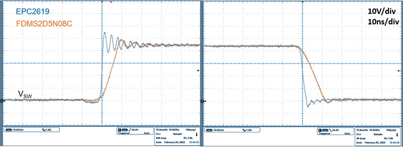
Switch node comparison at 15A (48 Vin, 12 Vout buck converter)
This can cause challenges during the measurement phase.
See AN023 Accurately Measuring High-Speed GaN Transistors for more details
Tips and tricks
GaN FETs high performance emphasizes the need for good measurement techniques for high-speed circuits.
- The ground loop should be minimized by utilizing a spring clip
- Probing location should be kept as close as possible to the device being tested
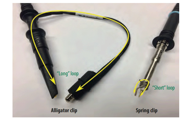
Example of probe grounding method
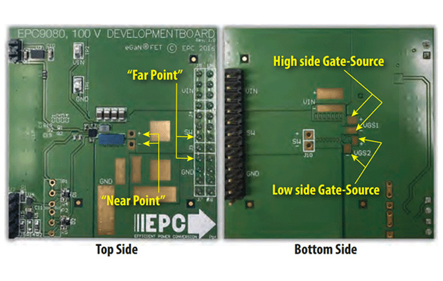
Example of "near" and "far" probing locations

Effect of probing techniques and choice of measurement point
Bandwidth requirements
If scopes or probes with insufficient bandwidth are used, then actual waveforms of a typical converter cannot be measured accurately. A 500MHz bandwidth is recommended for typical converters, and at least 1 GHz for some specific applications like LIDAR.
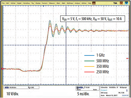
Effect of probe/system bandwidth on captured waveform (EPC9080 based board)
Differential probes
Of particular interest is the measurement of the high side gate in a typical half-bridge configuration. On top of the previous requirement in terms of bandwidth and measurement setup, this measurement presents additional requirements:
- Galvanic isolation: although the math channels can be used to reconstruct the high side gate, this method is susceptible to noise and mismatch between the two probes. A differential probe is recommended
- Large common mode rejection ratio (CMMR
- Common mode voltage rating > input voltage (Buck) or output voltage (Boost
- Large input impedance, preferably > 10 MΩ || < 2pF
Test equipment manufacturers have developed high performance differential probes suitable for this: for example Tektronix IsoVu, LeCroy DL-ISO, and PMK Firefly probes.
Double pulse measurements
This measurement method is commonly used to directly measure switching losses of semiconductor devices by using the math function of a scope to multiply the instantaneous voltage and current waveforms and then integrating them. The previous methods can be applied to measure the voltage, however measuring the current has these additional challenges:
- Bandwidth requirement: active current sensors struggle with the accuracy and bandwidth required, so current shunts are still the preferred method
- Current shunts require interrupting the power loop and inserting the sensor. The increase in power loop inductance can significantly change the measurement results
For these reasons EPC does not recommend double pulse testing, but rather utilizing Spice models (and a calibrated model if more accuracy is needed): EPC Device Models
Test equipment manufacturers are working on this topic, for example see the article Accurate Characterization of Low-Voltage, Small-Form–Factor GaN FETs.
Additional content
Resources
- How2AppNote – The Growing Ecosystem for GaN FET Power Conversion
- White Paper – eGaN FET Drivers and Layout Considerations
- Webinar: Gate Drivers for GaN FETs
- How to Design an eGaN FET-Based Power Stage with an Optimal Layout (How2AppNote007)
- Best Practices for Integrating eGaN FETs
- Impact of Parasitics on Performance (WP009)
- How2AppNote012 - How to Get More Power Out of an eGaN Converter
- Thermal Management of Chip-Scale Devices
- Improving Thermal Performance of Chip-Scale Packaged Gallium Nitride Transistors
- Webinar: Thermal Management of GaN FETs
For additional information on assembly guidelines, visit our page Assembly Resources.
GaN Talk Support Forum
- About the Designing with GaN FETs and ICs category
- EPC 23101 with the EPC 2306
- Altium file for EPC90123 dev board
- EPC2361 Altium Footprint
- EPC21603 V_Laser minimum
- Drain-source thermal resistance
- EPC2304 - KiCAD 9.0: No solder mask will be generated
- PLECS models for integrated driver + HB
- Apparent Shoot-Through Issue in LTSpice Simulation
- Using GaN Fet EPC2367 with the LM51772
Have a question about schematics and layout? Ask a GaN Expert
Buck Converters
| Imagem | Número de peça do fabricante | Descrição | Available Quantity | Ver detalhes | |
|---|---|---|---|---|---|
 |  | EPC9195 | BD REF DESIGN 48V/12V DC-DC | 9 - Immediate | Ver detalhes |
|  | EPC9158 | DCDC 48-12V/DUAL PHASE BUCK CONV | 20 - Immediate | Ver detalhes |
|  | EPC9157KIT | EVAL BOARD FOR EPC2218 | 20 - Immediate | Ver detalhes |
 | EPC9160 | DCDC 9-24V/DUALOUT 15A SYNC/BUCK | 10 - Immediate | Ver detalhes |
Boost Converters
| Imagem | Número de peça do fabricante | Descrição | Available Quantity | Ver detalhes | |
|---|---|---|---|---|---|
|  | EPC9166 | DCDC 500W DUAL PH/SYNCBOOST CONV | 10 - Immediate | Ver detalhes |
Buck or Boost Converters
| Imagem | Número de peça do fabricante | Descrição | Available Quantity | Ver detalhes | |
|---|---|---|---|---|---|
|  | EPC9165KIT | EVAL BOARD FOR EPC2302 | 19 - Immediate | Ver detalhes |
|  | EPC91106 | EVAL BOARD FOR EPC23104 | 17 - Immediate | Ver detalhes |
LLC full-bridge Converters
| Imagem | Número de peça do fabricante | Descrição | Available Quantity | Ver detalhes | |
|---|---|---|---|---|---|
|  | EPC9174KIT | REF DESN 1/8BRICK DCDC 1.2KW GAN | 18 - Immediate | Ver detalhes |
GaN-based Motor Drive Design Examples
| Imagem | Número de peça do fabricante | Descrição | Available Quantity | Ver detalhes | |
|---|---|---|---|---|---|
|  | EPC9193KIT | EVAL BOARD FOR EPC2619 | 23 - Immediate | Ver detalhes |
| | EPC9193HCKIT | EVAL BOARD FOR EPC2619 | 10 - Immediate | Ver detalhes |
|  | EPC9176KIT | EVAL BOARD FOR EPC23102 | 14 - Immediate | Ver detalhes |
|  | EPC9173KIT | BD REF GAN MOTOR CNTRLR/DRIVER | 21 - Immediate | Ver detalhes |
|  | EPC9194KIT | EVAL BOARD FOR EPC2302 | 3 - Immediate | Ver detalhes |
|  | EPC9186KIT | BD REF 3PH BLDC MOTR DRV 150ARMS | 24 - Immediate | Ver detalhes |
Lidar Evaluation Board Design Examples
| Imagem | Número de peça do fabricante | Descrição | Available Quantity | Ver detalhes | |
|---|---|---|---|---|---|
|  | EPC9144 | EVAL BOARD FOR EPC9144 | 25 - Immediate | Ver detalhes |
|  | EPC9154 | EVAL BOARD FOR EPC21601 | 30 - Immediate | Ver detalhes |
|  | EPC9156 | EVAL BOARD FOR EPC21603 | 17 - Immediate | Ver detalhes |
|  | EPC9172 | EVAL BOARD FOR EPC21701 | 0 - Immediate | Ver detalhes |
|  | EPC9179 | EVAL BOARD FOR EPC2252 | 25 - Immediate | Ver detalhes |
|  | EPC9181 | BD DEMO LIDAR HI CURENT EPC2204A | 10 - Immediate | Ver detalhes |
|  | EPC9180 | BD DEMO LIDAR HI CURENT EPC2218A | 13 - Immediate | Ver detalhes |
|  | EPC9150 | EVAL BOARD FOR EPC2034C | 26 - Immediate | Ver detalhes |
GaN Controllers for Buck and Boost Converters
| Imagem | Número de peça do fabricante | Descrição | Available Quantity | Ver detalhes | |
|---|---|---|---|---|---|
|  | MIC2128YML-TR | 75V, SYNCHRONOUS BUCK CONTROLLER | 1964 - Immediate | Ver detalhes |
|  | LTC7890RUJM#PBF | 100V DUAL SYNC BUCK CONTROLLER | 0 - Immediate | Ver detalhes |
|  | LTC7891RUFDM#TRPBF | IC REG BUCK | 1349 - Immediate | Ver detalhes |
|  | ISL81806FRTZ-T | 80V SYNC DUAL BUCK PWM CONTROLLE | 4457 - Immediate 21000 - Factory Stock | Ver detalhes |
| | ISL81807FRTZ-T | 80V SYNCHRONOUS DUAL BOOST PWM C | 4979 - Immediate 39000 - Factory Stock | Ver detalhes |
|  | MIC2132YML-TR | 75V, DUAL PHASE ADVANCED COT PWM | 0 - Immediate | Ver detalhes |
|  | RT6190GGQW | IC REG CTRLR BUCK-BOOST WQFN-40 | 1214 - Immediate | Ver detalhes |
|  | LT8390AEUFD#TRPBF | IC REG CTRLR BUCK-BOOST 28 | 1533 - Immediate | Ver detalhes |
|  | LM5141QRGETQ1 | IC REG CTRLR BUCK 24VGFN | 1194 - Immediate | Ver detalhes |
|  | LM5140RWGEVM | EVAL BOARD FOR LM5140Q1 | 4 - Immediate | Ver detalhes |
|  | DSPIC33CK32MP102-I/SS | IC MCU 16BIT 32KB FLASH 28SSOP | 1663 - Immediate | Ver detalhes |
|  | LTC7800EUDC#TRPBF | IC REG CTRLR SYNC BUCK 60V 20QFN | 1740 - Immediate | Ver detalhes |
|  | ISL8117AFRZ | IC REG CTRLR BUCK 16QFN | 0 - Immediate | Ver detalhes |
|  | TPS40400RHLR | IC REG CTRLR BUCK PMBUS 24QFN | 2221 - Immediate | Ver detalhes |
|  | BQ25770GREER | IC, 2-CELL TO 5-CELL, NVDC DUAL- | 2698 - Immediate | Ver detalhes |
|  | TPS53632GRSMT | IC REG CTRLR HALF-BRIDGE 32VQFN | 185 - Immediate 20000 - Marketplace | Ver detalhes |
 | NCP81118MNTWG | IC REG BUCK CTLR 36QFN | 0 - Immediate 125000 - Marketplace | Ver detalhes |
GaN Controllers for Synchronous Rectifiers
| Imagem | Número de peça do fabricante | Descrição | Available Quantity | Ver detalhes | |
|---|---|---|---|---|---|
|  | NCP4306AAAZZZADR2G | SECONDARY SIDE SYNCHRONOU | 11540 - Immediate | Ver detalhes |
|  | NCP43080DMTTWG | IC SECONDARY SIDE CTRLR 8WDFN | 2485 - Immediate | Ver detalhes |
|  | UCD7138DRST | IC GATE DRVR LOW-SIDE 6SON | 580 - Immediate 1000 - Marketplace | Ver detalhes |
|  | TEA1993TS/1H | IC CTRLR SYNC RECT SC-74 | 5892 - Immediate | Ver detalhes |
|  | TEA1995T/1J | IC CTRLR SYNC RECT 8SOIC | 5049 - Immediate | Ver detalhes |
Low-Side GaN Gate Drivers
| Imagem | Número de peça do fabricante | Descrição | Available Quantity | Ver detalhes | |
|---|---|---|---|---|---|
|  | 1EDB7275FXUMA1 | DIGITAL ISO 3KV 1CH GT DVR DSO8 | 5399 - Immediate | Ver detalhes |
|  | LMG1025-Q1EVM | EVAL BOARD FOR LMG1025-Q1 | 10 - Immediate | Ver detalhes |
Half-Bridge GaN Gate Drivers
| Imagem | Número de peça do fabricante | Descrição | Available Quantity | Ver detalhes | |
|---|---|---|---|---|---|
|  | 2EDB7259YXUMA1 | DGTL ISO 3KV 2CH GATE DVR DSO14 | 2281 - Immediate | Ver detalhes |
| | 2EDR7259XXUMA1 | DGTL ISO 5.7KV 2CH GT DVR DSO14 | 1018 - Immediate | Ver detalhes |
|  | NCP51810AMNTWG | IC GATE DRVR HALF-BRIDGE 15QFN | 1045 - Immediate | Ver detalhes |
|  | UP1966E | IC GATE DRVR HALF-BRIDGE 12WLCSP | 195639 - Immediate | Ver detalhes |
|  | ADUM4221ARIZ | IC GATE DRVR HALF-BRIDGE 16SOIC | 78 - Immediate | Ver detalhes |
|  | MP8699BGC-P | HALF-BRIDGE GAN MOSFET DRIVER | 0 - Immediate | Ver detalhes |
|  | STDRIVEG600 | IC HALF BRIDGE DRVR 5.5A/6A 16SO | 489 - Immediate | Ver detalhes |
GaN ICs for High Reliability Applications
| Imagem | Número de peça do fabricante | Descrição | Available Quantity | Ver detalhes | |
|---|---|---|---|---|---|
|  | FBS-GAM01P-C-PSE | SINGLE LOW SIDE DRIVER | 47 - Immediate | Ver detalhes |
|  | FBS-GAM02P-C-PSE | DUAL HIGH & LOW SIDE DRIVER | 9 - Immediate | Ver detalhes |
monolithic GaN integrated circuit
| Imagem | Número de peça do fabricante | Descrição | Available Quantity | Ver detalhes | |
|---|---|---|---|---|---|
| | UP1966E | IC GATE DRVR HALF-BRIDGE 12WLCSP | 195639 - Immediate | Ver detalhes |
|  | EPC21701 | IC GAN LASER DRVR 80V | 32889 - Immediate | Ver detalhes |
|  | EPC21603 | IC LASER DRVR 40V 10A LVDSLOGIC | 7674 - Immediate | Ver detalhes |
|  | EPC21601 | IC LASER DRVER 40V 10A 3.3VLOGIC | 9877 - Immediate | Ver detalhes |
|  | EPC2152 | IC HALF BRIDGE DRVR 12.5A 12LGA | 8314 - Immediate | Ver detalhes |
|  | EPC23101ENGRT | TRANS GAN 100V EPOWER STAGE | 4476 - Immediate | Ver detalhes |
|  | EPC23104ENGRT | IC HALF BRIDGE DRIVER 15A 13WQFN | 22887 - Immediate | Ver detalhes |
|  | EPC23102 | IC HALF BRIDGE DRIVER 35A 13WQFN | 8061 - Immediate | Ver detalhes |

